|
|
:: Faculty Labs (in alphabetical order)
- Majeed M Hayat's Laboratory

Degrees: PhD Electrical Engineering, University of Wisconsin-Madison, 1992 MS Electrical Engineering, University of Wisconsin-Madison, 1988 BS Electrical Engineering, University of the Pacific (Stockton, Calif.), 1985
Majeed Hayat has active research programs covering a broad range of topics in statistical communication theory, signal/image processing, photodetectors, optical communication, remote sensing, and distributed and cooperative networks. Dr. Hayat is best known for his pioneering work in modeling and understanding impact ionization and noise in avalanche-photodiode (APD) devices, which are used in optical receivers in telecommunications and deep space communication as well as in photon-starved infrared sensors. His work on modeling the stochastic process of carrier multiplication in APDs has significantly enhanced our understanding of how these devices behave, as well as how they perform in optical receivers and single-photon detectors. In 2007, Dr. Hayat spent his half-year sabbatical leave visiting his APD-research collaborators at the University of Sheffield, UK.
In the area of image processing, Hayat and his students have developed a number of key algorithms for nonuniformity correction for infrared thermal imagers. These algorithms, one of which has been patented and licensed to industry, remove what is called the fixed-pattern noise without the need for mechanical calibration mechanisms.
In 2007, Hayat and his collaborators (Santhanam, Gerstle, Simpson and Atwood, see page 24) led a new research initiative on developing a signal-processing method for combined imaging and vibrometry for synthetic aperture radar sensing platforms. This research has already received nearly $1.2M in funding from the departments of energy and defense. In the area of network modeling, Hayat and his collaborators (Bridges, Mostofi and Dietz) have received nearly $1.3M of basic research funding from the Defense Threat Reduction Agency’s program on combating weapons of mass destruction. This includes an $880,000 grant for the 2008 project titled “An Adaptive Probabilistic Approach for Maximal Reliability of Distributed Networks in the Presence of WMD Stressors.”
Dr. Hayat is a recipient of the NSF Early Faculty Career Award, ECE’s 2007 Outstanding Researcher Award, ECE’s 2005 Lawton-Ellis Award, and STC.UNM’s 2007 and 2008 Annual Creative Awards for issued U.S. Patents 7,132,648, 7,217,951 and 7,271,405. He is associate editor of Optics Express and chair of the Albuquerque Chapter for IEEE-LEOS. He currently supervises six doctoral students.
- Sanjay Krishna's Laboratory

Degrees:
PhD University of Michigan at Ann Arbor, 2001 MS Electrical Engineering, University of Michigan at Ann Arbor,1999 MSc Physics, Indian Institute of Technology, Madras, 1996 BSc (Hons) Physics, SSSIHL, Bangalore, India, 1994
Sanjay Krishna’s group proposed and pioneered the quantum dots in a well heterostructures (DWELL) for detectors in May 2002. The DWELL design combined the advantages of quantum well infrared photodetectors (QWIPs) such as a “dial in recipe” for a desired operating wavelength with the unique properties of quantum dot infrared photodetectors (QDIPs) such as low dark current and normal incidence operation. In addition, the DWELL design could exploit quantum confined Stark Effect (QCSE) due to the asymmetry of the potential, leading to the development of a “smart” focal plane array whose spectral response could be controlled using an external bias. A U.S. patent (Krishna et al. #7,217,951) was awarded for this work.
In the past few years, research groups around the world have investigated the DWELL design for intersubband detectors. This includes researchers at JPL, Northwestern University, Sheffield University Australian National University, University of Massachusetts and Mc- Master University. Recently, the DWELL detectors were successfully transitioned to NASA-JPL, where the demonstration of the largest QD based imager using a 640x512 focal plane array was undertaken. Although there is a fair amount of research to be done to reduce the dark current and increase the operating temperature of QD based devices, the DWELL design is a promising approach to realize next generation infrared imagers.
Dr. Krishna is co-founder of ECE’s Expand Your Engineering Skills (EYES) program, which brings high-caliber international students to ECE for summer research under the guidance of a faculty advisor (see page 29). He is the recipient of the Gold Medal from IIT and an IEEE Outstanding Engineer Award.
- Luke Lester's Laboratory

Degrees: PhD Electrical Engineering, Cornell University, 1992 BS Engineering Physics, Cornell University, 1984
Luke Lester has five U.S. and international patents and one patent pending in the fields of quantum dot “DWELL” technology and midinfrared semiconductor laser technology.
He teaches courses in optoelectronics, semiconductor lasers, semiconductor physics, microelectronics processing, and semiconductor materials and devices, and he currently serves as major advisor to ten students. He is the co-chair of the Optical Science and Engineering program at UNM.
He contributed to quantum-dot research that led to the development of a semiconductor laser with a lower threshold current, purer signal, and wider-wavelength range of operation than any other existing semiconductor laser. In 2001 he co-founded Zia Laser, Inc. to commercialize this technology and served as the company’s chief technical officer for two years. The company was purchased by Innolume GmbH in November 2006.
Promoted by ECE to full professor in 2007, Dr. Lester received ECE’s Excellence in Teaching Award in 2007 and the School of Engineering’s Junior Faculty Research Award in 1997.
Dr. Lester received a UNM University Libraries faculty acknowledgement award in 2006 “for his scholarly achievement and exemplary contributions to the School of Engineering.” He was also awarded an Air Force Summer Faculty Fellowship in 2006 and 2007.
A senior member of IEEE, Dr. Lester has published more than 150 journal articles, conference presentations and invited papers, and his work is estimated to have at least 1,800 citations.
- Marek Osinski's Laboratory

Degrees: PhD, Physical Sciences, Institute of Physics, Polish Academy of Science, Warsaw, Poland, 1979 MS, Physics, University of Warsaw, Poland, 1971
As program director of UNM’s $3.1 million fellowship program on Integrating Nanotechnology with Cell Biology and Neuroscience, one of Marek Osinski’s current focuses is to develop applications of rapidly evolving nanotechnologies to cell biology and neuroscience. An NSFfunded Integrated Graduate Education Research Traineeship (IGERT) program, the fellowship has supported 16 PhD students since 2006 with generous $30,000 a year stipends. The program also has an international component, supporting extended visits by the Fellows to Germany and Australia.
Dr. Osinski’s research interests include synthesis and characterization of colloidal nanocrystals, biomedical applications of colloidal quantum dots, nuclear radiation detectors (and nanoscintillators in particular), development of semiconductor ring-laser-based rotation sensors, fast/ slow light in semiconductor structures, ultrafast optoelectronic integrated circuits, modeling and simulation of optoelectronic devices, and growth and properties of novel optoelectronic materials.
A Fellow of the Society for Photo-Optical Instrumentation Engineers (SPIE) and of the Optical Society of America, Dr. Osinski has chaired or co-chaired 29 SPIE conferences and symposia, edited 24 SPIE Proceedings volumes, and served on numerous conference program committees. He has authored or co-authored more than 415 technical papers and five book chapters, and he holds five patents.
Dr. Osinski holds joint professorships with UNM’s Physics & Astronomy and Computer Science departments. He is also an ECE member of the Optical Science and Engineering Graduate Committee, the governing body of the OSE program.
- Ganesh Balakrishnan's Laboratory
Degrees:
PhD, Optical Sciences and Engineering, UNM, 2006
MS, Electrical Engineering, University of Toledo, Toledo, Ohio, 2001
BE, Electronics and Communications, University of Madras, India, 2000
Ganesh Balakrishnan was the technical director of the Integrated Nanomaterials core facility at the California Nano- Systems Institute at the University of California at Los Angeles from 2007 to 2008. He was responsible for conducting III-V optoelectronic, III-V/silicon integration and nanotechnology research.
Prior to 2007 he was a postdoctoral researcher at UNM’s Center for High Technology Materials, where he worked extensively on the epitaxial development of antimonide semiconductors on GaAs and silicon substrates. His accomplishments during that time included the first demonstration of communication wavelength laser diodes on Si substrate and the longest wavelength diode lasers on GaAs (up to 2 µm).
His present research interests include III-V based optoelectronics, including epitaxy, characterization, microscopy and device fabrication with a focus on lasers.
Dr. Balakrishnan has produced 25 publications in peer reviewed journals, with five more publications currently in review. He has made 13 conference presentations as a speaker and 31 conference presentations as a contributing author, and he chaired conference sessions at the Electronics Materials Conference 2007 and the North American MBE conference (NAMBE) 2007.
He has filed for seven patents, with three converted and four in provisional stage.
- Steven Brueck's Laboratory
Degrees:
PhD, Electrical and Computer Engineering, Massachusetts Institute of Technology, 1971 MS, Electrical Engineering, Massachusetts Institute of Technology, 1967 BS, Electrical Engineering, Columbia University, 1965
Steve Brueck was the first professor in the hundred-year history of the School of Engineering to be named a UNM Distinguished Professor, in 2006. The title, now held by four professors in the School, is the highest UNM bestows on its faculty.
Dr. Brueck has provided both technical and administrative leadership as director of UNM’s Center for High Technology Materials since joining ECE in 1985. Generating more than $9 million annually in grants and contracts, CHTM is an internationally recognized center for optoelectronics, microelectronics and nanotechnology research.
Dr. Brueck is the founding editor of the IEEE Journal of Special Topics in Quantum Electronics. In 1991 he received the UNM School of Engineering’s Outstanding Researcher Award, and in 2000 IEEE awarded him the Third Millennium Medal.
Dr. Brueck’s research explores the extension of optical lithography/ microscopy to the high-resolutions necessary for future generations of ICs. He applies the capabilities of interferometric lithography to expand nanophotonic, nanoscale growth and nanofluidic science and technology. A topic of recent interest is extending microscopy, one of the oldest and most important areas of optical science, to higher resolutions approaching the linear systems limits.
He currently is faculty advisor to seven doctoral students and three postdoctoral/senior scientists, and he holds a joint appointment in UNM’s Physics & Astronomy Department.
- Christos Chritodoulou's Laboratory
Degrees: PhD Electrical Engineering, North Carolina State University at Raleigh, 1985 MS Electrical Engineering, North Carolina State University at Raleigh, 1981 BS Physics with Solid State Electronics option, American University in Cairo, Egypt, 1979
Research Interests Wireless communications, numerical techniques in electromagnetics, smart antennas, neural network and machine learning applications in electromagnetics, reconfigurable antennas, RF/photonic antennas.
Plenary Speaker 2007 SBMO/IEEE MTT-S International Microwave & Optoelectronics Conference (IMOC 2007), Salvador, Brazil, Oct. 2007.
Notable Professional Activities
• Keynote speaker in the 2007 International Workshop & Expo on Anti-counterfeiting, Security, Identification; Xiamen, China, April 2007 • Editor of a special issue on “Synthesis and Optimization Techniques in Electromagnetics and Antenna System Design”, IEEE Transactions on Antennas and Propagation, 2007 • Taught a two-week course on antennas at Jiao Tong University in Shanghai, May 2007 • Gave talks as the IEEE APS Distinguished Speaker in Cleveland (NASA/ Case Western Reserve University), Los Angeles, and Toronto IEEE Chapters as well as at the universities of Sabanci, Koch, Bilkent and METU in Turkey and the Democritus University of Xanthi in Greece • Tau Beta Pi Advisor 2007-present; elected Senate Committee member • Vice chair of IEEE Albuquerque Section • Member of the Technical Committee Programs for IMOC, Brazil 2007; HUT-ICCE, Hanoi-Vietnam 2008; MAPE 2007, Hangzhou, China 2007; LAPC, UK 2008; IEEE AP, Hawaii 2007; and IEEE APS Conference in San Diego 2008
- Daniel Feezell

Prior to joining UNM, Daniel Feezell was a Project Scientist in the Solid-State Lighting and Energy Center at the University of California Santa Barbara (UCSB) from 2010-2012. Working in the research group of Prof. Shuji Nakamura, he directed projects on nonpolar and semipolar light-emitting diodes (LEDs) and laser diodes. A significant accomplishment during this period includes the first demonstration of a nonpolar GaN-based vertical-cavity surface-emitting laser. From 2008-2010, Dr. Feezell was a Senior Device Scientist and the first employee at Kaai/Soraa, Inc., where he developed high-performance GaN-based laser diodes and LEDs.
Dr. Feezell received the Ph.D. degree in 2005 under the direction of Prof. Larry Coldren at the University of California Santa Barbara. He developed monolithic 1.31 – 1.55 µm InP- based vertical-cavity surface-emitting lasers with novel optical apertures, leading to differential efficiencies above 60%. From 2005-2008, Dr. Feezell held a postdoctoral position at UCSB developing nonpolar GaN-based laser diodes. For his role in the achievement of the first nonpolar GaN-based edge-emitting laser diodes he received the 30th Annual Japanese Journal of Applied Physics Paper Award. He is the author or co-author of more than 50 peer-reviewed conference and journal publications, and has received several patents.
Research Interests:
Epitaxial growth, fabrication, and characterization of group III-nitride materials and devices, including nonpolar/semipolar orientations. Solid-state lighting and high-efficiency LEDs. Visible edge-emitting and vertical-cavity surface-emitting lasers. Applications of group III-nitrides to energy efficiency and renewable energy.
- Charles Fleddermann
Degrees: PhD Electrical Engineering, University of Illinois at Urbana-Champaign, 1985 MS Electrical Engineering, University of Illinois at Urbana-Champaign, 1980 BS Electrical Engineering, University of Notre Dame, 1977
Dr. Fleddermann is UNM’s Acting Dean of Graduate Studies as well as the School of Engineering’s Associate Dean for Academic Affairs, a post he has held since 2002.
Dr. Fleddermann is principal investigator on a $1.8 million NSF grant for 2004-08 to train and send graduate teaching fellows into Albuquerque’s West Mesa secondary and elementary schools. The fellows’ objective is to boost both learning and teaching of math and science with lessons in optics and photonics.
Dr. Fleddermann developed an engineering ethics course for ECE in response to the ABET standard of incorporating ethics topics into the undergraduate engineering curriculum. His 1999 undergraduate textbook, Engineering Ethics, now in its third edition, is used by a number of universities nationally and internationally. It addresses the ways in which technology raises ethical concerns for engineers and how engineers can avoid ethical problems before they happen. Dr. Fleddermann also teaches professional development courses on engineering ethics in partnership with the New Mexico Society of Professional Engineers.
His main research area is plasma processing of semiconductor materials, which involves using ionized gases to pattern transistors and other electronic devices during the manufacturing of integrated circuits such as microprocessor chips.
- Nazir Ghani
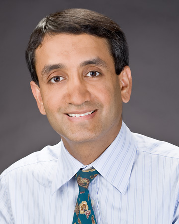
Degrees: PhD, University of Waterloo, Canada, 1997 ME EE, McMaster University, Canada, 1992 BE, Computer Engineering, University of Waterloo, Canada, 1991
Dr. Ghani has gained a wide range of academic and industrial experience in the telecommunications field. Prior to joining UNM he was an associate professor in ECE at Tennessee Tech University and also held a joint position as a Collaborating Scientist at Oak Ridge National Lab. In the past he has also held senior technical positions at Nokia, IBM, Motorola and Sorrento Networks. Dr. Ghani has made significant contributions in optical networking, and his earlier work on IP-optical integration was one of the first to develop a comprehensive control architecture for modern transport networks. He has published more than 100 archival publications (including journals, conferences, book chapters, and standardization contributions) and holds two U.S. patents. He is a recipient of the NSF CAREER Award and is a Senior Member of the IEEE. Dr. Ghani is advising several doctoral students and teaches courses in networking and software engineering. He is also involved with various high-school outreach activities.
Current Research
Dr. Ghani has built an advanced High Speed Networks Laboratory at UNM, and his current research interests include network virtualization and services, hybrid inter-networking and metro/access networks. He is actively funded by several large grants from the NSF and Department of Energy Office of Science, focusing on the design of new architectures and algorithms for multi-domain, multi-layer networks.
- Mani Hossein-Zadeh
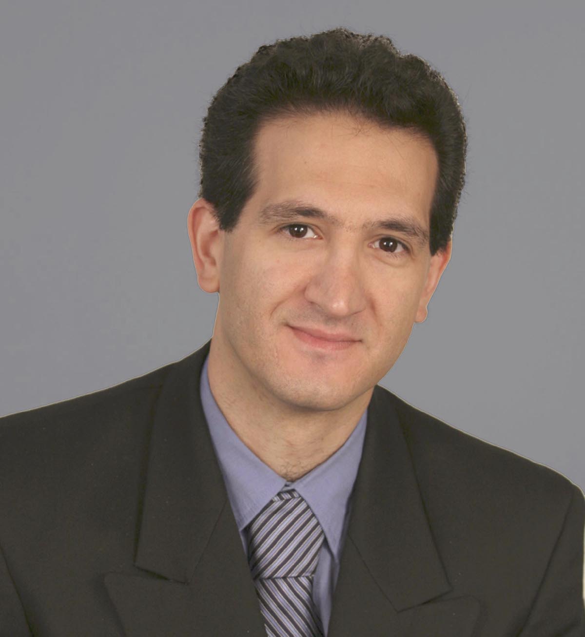
Degrees: PhD, Electrical Engineering, University of Southern California (USC), Los Angeles, 2004 MS, Electrical Engineering, USC, 2001 MS, Physics, Sharif University of Technology, Tehran, 1997 BS, Applied Physics, Sharif University of Technology, 1995
Mani Hossein-Zadeh previously held a postdoctoral appointment with the Applied Physics department at the California Institute of Technology, where he worked on fluidic optical resonators, optomechanical oscillators, free microtoroid optical resonators and optomechanical interaction in ultra-high-Q (UH-Q) optical microresonators. His work on free microtoroids has demonstrated the possibility of employing UH-Q optical microtoroid resonators in different photonic platforms. He has characterized different aspects of the first optomechanical RF oscillator and demonstrated its application in RF-photonics.
During his PhD studies at the Viterbi School of Engineering at USC he made major contributions in developing the first high-Q electro-optic microdisk modulator and designed and demonstrated the first photonic RF receiver based on this device.
Dr. Hossein-Zadeh received a two-year postdoctoral fellowship from the Center for Physics of Information at Caltech. His work on photonic microdisk RF receivers and UH-Q microtoroid resonators has been funded by the Army Research Office (DARPA), NASA, Hughes Research Laboratories and NSF.
His interests include photonic/microwave-photonic devices and their application in communication, signal processing, biophysics and fundamental physics. Specifically he is interested in exploring the physics and applications of high-Q optical Whispering-Gallery microresonators.
- Ravinder K.Jain
Degrees: PhD, EECS, University of California, Berkeley,1974 MS, EECS, University of California, Berkeley,1972 BS, EE, University of California, Santa Barbara, 1970 AB, Physics, University of California, Santa Barbara, 1970
Ravi Jain has made pioneering contributions to several areas of fundamental and applied physics and laser engineering. His scientific contributions have included the first experimental studies of the feasibility of laser-induced optical (anti-Stokes) cooling, the first proposal and elucidation of the plasmon-photon interaction in tunnel junctions, and numerous valuable studies on nonlinear optical interactions in glass fibers and in semiconductors, including quantum-confined semiconductor nanoparticles and coupled quantum dot metallic nanoparticle assemblies.
His engineering contributions have included the invention and demonstration of the cw tunable fiber Raman oscillator, the synchronously mode-locked cw dye laser, non-invasive optical probes for high-speed integrated circuits, and a large range of fiber lasers for telecom applications and for efficient visible upconversion and mid-IR downconversion sources. Most notable among the latter is his group’s recent demonstration of very high efficiency mid-infrared fiber lasers with power outputs of several watts, over 4 orders of magnitude higher than those demonstrated previously in the literature. These mid-IR fiber lasers have strong potential as compact field-usable tunable sources for trace level (sub-ppb) sensors of several molecular species, and as replacements of the conventional Er:YAG laser for numerous surgical applications ranging from dermatology to otology and ophthalmology.
- Edl Schamiloglu
Degrees:
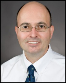
PhD Applied Physics, Cornell University, Ithaca, NY, 1988 MS Columbia University, New York City, 1981 BS Columbia University, New York City, 1979
Edl Schamiloglu’s group is actively working on their $1.2M ONR grant, awarded in 2006. This is a collaborative effort with professors Christodoulou and Gilmore and with the University of Michigan and SAIC.
Professor Schamiloglu presented invited talks describing this research at the BEAMS Conference in Xi’an, China, and at the EUROEM Conference in Lausanne, Switzerland, both in July 2008. Professor Schamiloglu’s research is also supported by a new three-year grant from AFOSR (together with Professor Gilmore, and supplemented by a 2008 DURIP Instrumentation Grant) that focuses on minimizing surface plasmas within high-power microwave sources.
A recent trend in Professor Schamiloglu’s research is increased support from industry. He has support from Ktech Corporation to study frequency-tunable relativistic backward-wave oscillators, and he has an STTR with Sienna Technologies to develop novel high dielectric constant polymers for pulsed power applications.
|


